- 您现在的位置:买卖IC网 > Sheet目录1214 > EVAL-ADM1166TQEBZ (Analog Devices Inc)BOARD EVAL FOR ADM1166TQ
�� �
�
�ADM1166�
�The� device� also� has� several� identification� registers� (read-only)�
�that� can� be� read� across� the� SMBus.� Table� 12� lists� these� registers�
�with� their� values� and� functions.�
�All� other� devices� on� the� bus� remain� idle� while� the� selected�
�device� waits� for� data� to� be� read� from� or� written� to� it.� If� the�
�R/W� bit� is� a� 0,� the� master� writes� to� the� slave� device.� If� the�
�Table� 12.� Identification� Register� Values� and� Functions�
�Name� Address� Value� Function�
�MANID� 0xF4� 0x41� Manufacturer� ID� for� Analog�
�Devices�
�REVID� 0xF5� 0x02� Silicon� revision�
�MARK1� 0xF6� 0x00� Software� brand�
�MARK2� 0xF7� 0x00� Software� brand�
�General� SMBus� Timing�
��read� and� write� operations� using� the� SMBus.� The� SMBus� specification�
�defines� specific� conditions� for� different� types� of� read� and� write�
�operations,� which� are� discussed� in� the� Write� Operations� and� the�
�Read� Operations� sections.�
�The� general� SMBus� protocol� operates� in� the� following� three� steps.�
�2.�
�R/W� bit� is� a� 1,� the� master� reads� from� the� slave� device.�
�Data� is� sent� over� the� serial� bus� in� sequences� of� nine� clock�
�pulses:� eight� bits� of� data� followed� by� an� acknowledge� bit�
�from� the� slave� device.� Data� transitions� on� the� data� line�
�must� occur� during� the� low� period� of� the� clock� signal� and�
�remain� stable� during� the� high� period� because� a� low-to-high�
�transition� when� the� clock� is� high� could� be� interpreted� as� a�
�stop� signal.� If� the� operation� is� a� write� operation,� the� first�
�data� byte� after� the� slave� address� is� a� command� byte.� This�
�command� byte� tells� the� slave� device� what� to� expect� next.� It�
�may� be� an� instruction� telling� the� slave� device� to� expect� a�
�block� write,� or� it� may� be� a� register� address� that� tells� the�
�slave� where� subsequent� data� is� to� be� written.� Because� data�
�can� flow� in� only� one� direction,� as� defined� by� the� R/W� bit,�
�sending� a� command� to� a� slave� device� during� a� read� operation�
�is� not� possible.� Before� a� read� operation,� it� may� be� necessary�
�1.�
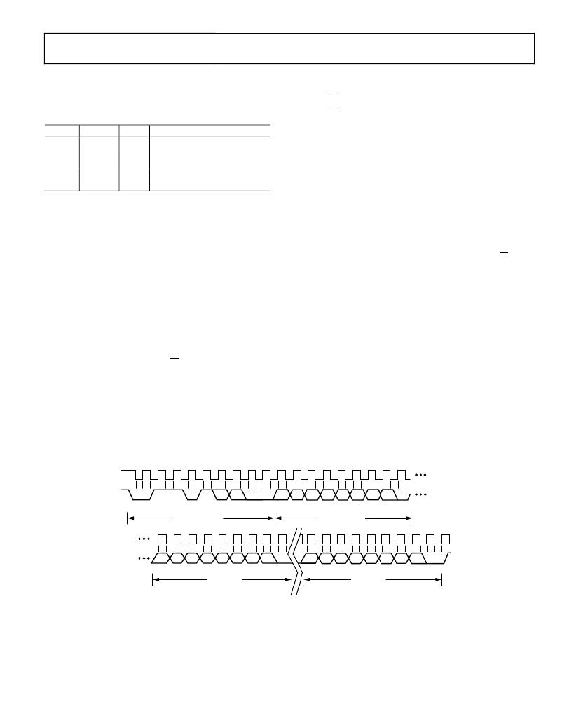
�The� master� initiates� data� transfer� by� establishing� a� start�
�condition,� defined� as� a� high-to-low� transition� on� the� serial�
�data� line� SDA,� while� the� serial� clock� line� SCL� remains� high.�
�This� indicates� that� a� data� stream� follows.� All� slave� peripherals�
�connected� to� the� serial� bus� respond� to� the� start� condition�
�and� shift� in� the� next� eight� bits,� consisting� of� a� 7-bit� slave�
�address� (MSB� first)� plus� an� R/W� bit.� This� bit� determines�
�the� direction� of� the� data� transfer,� that� is,� whether� data� is�
�written� to� or� read� from� the� slave� device� (0� =� write,� 1� =� read).�
�The� peripheral� whose� address� corresponds� to� the� transmitted�
�address� responds� by� pulling� the� data� line� low� during� the�
�low� period� before� the� ninth� clock� pulse,� known� as� the�
�3.�
�to� perform� a� write� operation� to� tell� the� slave� what� sort� of�
�read� operation� to� expect� and/or� the� address� from� which�
�data� is� to� be� read.�
�When� all� data� bytes� have� been� read� or� written,� stop� conditions�
�are� established.� In� write� mode,� the� master� pulls� the� data� line�
�high� during� the� 10� th� clock� pulse� to� assert� a� stop� condition.�
�In� read� mode,� the� master� device� releases� the� SDA� line� during�
�the� low� period� before� the� ninth� clock� pulse,� but� the� slave� device�
�does� not� pull� it� low.� This� is� known� as� a� no� acknowledge.�
�The� master� then� takes� the� data� line� low� during� the� low�
�period� before� the� 10� th� clock� pulse� and� then� high� during� the�
�10� th� clock� pulse� to� assert� a� stop� condition.�
�acknowledge� bit,� and� by� holding� it� low� during� the� high� period�
�of� this� clock� pulse.�
�1�
�9�
�1�
�9�
�SCL�
�SDA�
�0�
�1�
�1�
�0�
�1�
�A1�
�A0�
�R/W�
�D7�
�D6�
�D5�
�D4�
�D3�
�D2�
�D1�
�D0�
�START� BY�
�MASTER�
�FRAME� 1�
�SLAVE� ADDRESS�
�ACK.� BY�
�SLAVE�
�FRAME� 2�
�COMMAND� CODE�
�ACK.� BY�
�SLAVE�
�1�
�9�
�1�
�9�
�SCL�
�(CONTINUED)�
�SDA�
�(CONTINUED)�
�D7�
�D6�
�D5�
�D4�
�D3�
�D2�
�D1�
�D0�
�D7�
�D6�
�D5�
�D4�
�D3�
�D2�
�D1�
�D0�
�ACK.� BY�
�ACK.� BY�
�STOP�
�FRAME� 3�
�DATA� BYTE�
�SLAVE�
�FRAME� N�
�DATA� BYTE�
�SLAVE�
�BY�
�MASTER�
�Figure� 36.� General� SMBus� Write� Timing� Diagram�
�Rev.� 0� |� Page� 27� of� 32�
�发布紧急采购,3分钟左右您将得到回复。
相关PDF资料
EVAL-ADM1168LQEBZ
BOARD EVAL FOR ADM1168LQ
EVAL-ADM1170EBZ
BOARD EVALUATION FOR ADM1170
EVAL-ADM1171EBZ
BOARD EVALUATION FOR ADM1171
EVAL-ADM1172EBZ
BOARD EVALUATION FOR ADM1172
EVAL-ADM1175EBZ
BOARD EVALUATION FOR ADM1175
EVAL-ADM1176EBZ
BOARD EVALUATION FOR ADM1176
EVAL-ADM1177EBZ
BOARD EVALUATION FOR ADM1177
EVAL-ADM1178EBZ
BOARD EVALUATION FOR ADM1178
相关代理商/技术参数
EVAL-ADM1168LQEBZ
功能描述:BOARD EVAL FOR ADM1168LQ RoHS:是 类别:编程器,开发系统 >> 评估演示板和套件 系列:* 标准包装:1 系列:- 主要目的:电信,线路接口单元(LIU) 嵌入式:- 已用 IC / 零件:IDT82V2081 主要属性:T1/J1/E1 LIU 次要属性:- 已供物品:板,电源,线缆,CD 其它名称:82EBV2081
EVAL-ADM1169LQEBZ
功能描述:BOARD EVAL FOR ADM1169LQ RoHS:是 类别:编程器,开发系统 >> 评估演示板和套件 系列:Super Sequencer® 标准包装:1 系列:PSoC® 主要目的:电源管理,热管理 嵌入式:- 已用 IC / 零件:- 主要属性:- 次要属性:- 已供物品:板,CD,电源
EVAL-ADM1170EBZ
功能描述:BOARD EVALUATION FOR ADM1170 RoHS:是 类别:编程器,开发系统 >> 评估演示板和套件 系列:- 标准包装:1 系列:- 主要目的:电信,线路接口单元(LIU) 嵌入式:- 已用 IC / 零件:IDT82V2081 主要属性:T1/J1/E1 LIU 次要属性:- 已供物品:板,电源,线缆,CD 其它名称:82EBV2081
EVAL-ADM1171EBZ
功能描述:BOARD EVALUATION FOR ADM1171 RoHS:是 类别:编程器,开发系统 >> 评估演示板和套件 系列:- 标准包装:1 系列:- 主要目的:电信,线路接口单元(LIU) 嵌入式:- 已用 IC / 零件:IDT82V2081 主要属性:T1/J1/E1 LIU 次要属性:- 已供物品:板,电源,线缆,CD 其它名称:82EBV2081
EVAL-ADM1172EBZ
功能描述:BOARD EVALUATION FOR ADM1172 RoHS:是 类别:编程器,开发系统 >> 评估演示板和套件 系列:- 标准包装:1 系列:- 主要目的:电信,线路接口单元(LIU) 嵌入式:- 已用 IC / 零件:IDT82V2081 主要属性:T1/J1/E1 LIU 次要属性:- 已供物品:板,电源,线缆,CD 其它名称:82EBV2081
EVAL-ADM1175EBZ
功能描述:BOARD EVALUATION FOR ADM1175 RoHS:是 类别:编程器,开发系统 >> 评估演示板和套件 系列:- 标准包装:1 系列:- 主要目的:电信,线路接口单元(LIU) 嵌入式:- 已用 IC / 零件:IDT82V2081 主要属性:T1/J1/E1 LIU 次要属性:- 已供物品:板,电源,线缆,CD 其它名称:82EBV2081
EVAL-ADM1176EBZ
功能描述:BOARD EVALUATION FOR ADM1176 RoHS:是 类别:编程器,开发系统 >> 评估演示板和套件 系列:- 标准包装:1 系列:- 主要目的:电信,线路接口单元(LIU) 嵌入式:- 已用 IC / 零件:IDT82V2081 主要属性:T1/J1/E1 LIU 次要属性:- 已供物品:板,电源,线缆,CD 其它名称:82EBV2081
EVAL-ADM1177EBZ
功能描述:BOARD EVALUATION FOR ADM1177 RoHS:是 类别:编程器,开发系统 >> 评估演示板和套件 系列:- 标准包装:1 系列:- 主要目的:电信,线路接口单元(LIU) 嵌入式:- 已用 IC / 零件:IDT82V2081 主要属性:T1/J1/E1 LIU 次要属性:- 已供物品:板,电源,线缆,CD 其它名称:82EBV2081